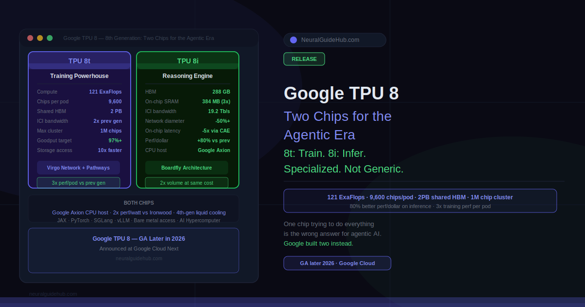
For most of the past decade, a single TPU architecture had to do everything. Train the model. Serve the model. Handle the inference. Make it fast enough, power-efficient enough, and scalable enough across all of those very different workloads. That worked when AI looked like “run a prompt, get a response.” It stops working when AI looks like “run 300 agents simultaneously through a 13-hour autonomous workflow.” Google’s answer to that problem is the Google TPU 8 generation, announced at Google Cloud Next, and the core decision is splitting into two distinct chips: TPU 8t for training and TPU 8i for inference.
This is not just a performance bump on the previous generation. It is a rethinking of what the chips need to do, based on what AI workloads now actually look like in production.
Why Two Chips Instead of One
The reasoning is straightforward once you understand the workload difference. Training is compute-bound. You need maximum throughput, scale-up bandwidth, and the ability to keep thousands of chips busy processing a massive dataset for weeks without significant downtime. Inference is memory-bound. You need low latency, fast access to the model’s working state, and the ability to handle thousands of simultaneous agent interactions without each one waiting on the others.
Optimizing a single chip for both requires compromising on both. Google identified this several years ago when they anticipated that inference demand would grow as frontier models moved into production. The agentic era accelerated the urgency. When agents run in continuous loops — reasoning, planning, executing, learning, repeating — even small latency inefficiencies compound across thousands of agent interactions simultaneously.
The result is two chips that can both technically run either workload, but are each specialized enough that the specialization delivers meaningful efficiency gains over a generalist design.
Google TPU 8t: The Training Architecture
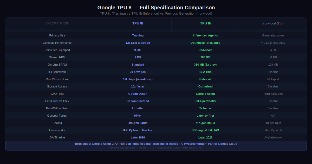
TPU 8t is built to compress frontier model development timelines. The headline number is 121 ExaFlops of compute per superpod, nearly 3x the compute performance of the previous generation per pod. A single TPU 8t superpod scales to 9,600 chips with two petabytes of shared high bandwidth memory and double the interchip bandwidth of the generation before.
Those numbers matter most at scale. Two petabytes of shared HBM means the most complex models can use a single, massive pool of memory rather than constantly moving data between partitioned memory spaces. Double the interchip bandwidth means the chips spend more time computing and less time waiting for data to arrive from neighboring chips.
The storage access improvement is 10x faster than previous generations, combined with TPUDirect pulling data directly into the chip rather than routing through CPU memory. Both are aimed at the same problem: keeping the chips busy rather than waiting.
The Virgo Network fabric enables near-linear scaling up to one million chips in a single logical cluster. That is not a theoretical ceiling. It is the architecture target. Training runs that currently require careful partitioning across separate clusters can run as one coherent system.
Google is targeting over 97% “goodput” on TPU 8t, which is the percentage of time the cluster is doing useful training work rather than recovering from failures, rerouting around faults, or waiting on checkpoint restarts. At frontier training scale, a one percent drop in goodput translates to days of lost compute time across a training run. The reliability engineering baked into TPU 8t, including real-time telemetry across tens of thousands of chips and automatic fault rerouting via Optical Circuit Switching, is specifically designed to protect that number.
Google TPU 8i: The Inference Architecture
TPU 8i is designed around a different problem. In agentic workflows, many specialized agents run simultaneously, often coordinating with each other in complex flows. The latency of each individual step multiplies across the coordination overhead. A chip optimized for raw training throughput will bottleneck on the memory access patterns that inference and multi-agent coordination require.
The memory architecture is the centerpiece. TPU 8i carries 288 GB of high-bandwidth memory paired with 384 MB of on-chip SRAM, which is 3x more than the previous generation. The goal is keeping a model’s active working state entirely on-chip rather than constantly pulling from external HBM. When the data the chip needs is already on-chip, the latency of memory access drops dramatically.
For Mixture of Experts models specifically, which dominate the current generation of frontier models, TPU 8i doubles the Interconnect bandwidth to 19.2 Tb/s. The Boardfly architecture reduces the maximum network diameter by more than 50%, which reduces the distance data has to travel between chips during MoE routing. Less distance means less latency means faster token generation per agent interaction.
The on-chip Collectives Acceleration Engine offloads global communication operations from the main compute units, reducing on-chip latency by up to 5x. In practice, this targets the “waiting room” problem: processors sitting idle while global operations complete before the next compute step can start.
The efficiency result is 80% better performance-per-dollar over the previous generation. Google claims this enables serving nearly twice the customer volume at the same cost. For enterprises running production inference at scale, that number has direct budget implications.
Co-Designed with Gemini, Available to Everyone
Both chips run natively on Google’s own Axion ARM-based CPU host, which is the first time a TPU generation has used Google’s own processor rather than third-party CPU hardware. Owning the CPU host alongside the accelerator allows system-level optimization that is not possible when the two are designed independently. Power management, memory architecture, and thermal management can all be co-optimized at the full system level.
The co-design with Google DeepMind is explicit in the spec decisions. The Boardfly topology was designed for the communication patterns of reasoning models. The SRAM capacity in TPU 8i was sized for the KV cache footprint of reasoning models at production scale. The Virgo Network bandwidth targets came from the parallelism requirements of trillion-parameter training. These are not general-purpose decisions. They are decisions derived from the specific demands of frontier models.
Both platforms support native JAX, MaxText, PyTorch, SGLang, and vLLM, which covers the frameworks most AI teams already use. Bare metal access gives customers direct hardware access without virtualization overhead. Open-source contributions including MaxText reference implementations and Tunix for reinforcement learning are available alongside the hardware.
Power Efficiency at Data Center Scale
Both chips deliver up to 2x better performance-per-watt over the previous Ironwood generation. Google integrates network connectivity with compute on the same chip, reducing the power cost of moving data across the TPU pod. The fourth-generation liquid cooling technology sustains performance densities that air cooling cannot support at the power levels these chips require.
Google’s data centers now deliver six times more computing power per unit of electricity than they did five years ago. TPU 8t and TPU 8i continue that trajectory. At the scale Google operates, efficiency is not just an environmental consideration. It is a hard operational constraint. Power availability limits what can be built and operated, and chip-level efficiency directly determines what is possible within those power envelopes.
TPU 8t and TPU 8i will be generally available later in 2026. Both chips are part of Google’s AI Hypercomputer, which combines purpose-built hardware with open software frameworks and flexible consumption models into a unified stack. Citadel Securities is among the early organizations already using TPUs for production AI workloads. Interested customers can request more information through Google Cloud.
The broader implication of this release is architectural. The agentic era changes what infrastructure needs to do, and a single chip designed to handle everything adequately is a worse answer than two chips designed to handle their respective workloads well. That trade-off is what TPU 8t and TPU 8i represent.